

Abstract
Two-dimensional electronic states at surfaces are often observed in simple wide-band metals such as Cu or Ag (refs. 1,2,3,4).nanomet监禁的封闭几何图形re scale, such as surface terraces, leads to quantized energy levels formed from the surface band, in stark contrast to the continuous energy dependence of bulk electron bands2,5,6,7,8,9,10。Their energy-level separation is typically hundreds of meV (refs. 3,6,11).在一个不同的类材料,strong electronic correlations lead to so-called heavy fermions with a strongly reduced bandwidth and exotic bulk ground states12,13。Quantum-well states in two-dimensional heavy fermions (2DHFs) remain, however, notoriously difficult to observe because of their tiny energy separation. Here we use millikelvin scanning tunnelling microscopy (STM) to study atomically flat terraces on U-terminated surfaces of the heavy-fermion superconductor URu2Si2, which exhibits a mysterious hidden-order (HO) state below 17.5 K (ref. 14).We observe 2DHFs made of 5f electrons with an effective mass 17 times the free electron mass. The 2DHFs form quantized states separated by a fraction of a meV and their level width is set by the interaction with correlated bulk states. Edge states on steps between terraces appear along one of the two in-plane directions, suggesting electronic symmetry breaking at the surface. Our results propose a new route to realize quantum-well states in strongly correlated quantum materials and to explore how these connect to the electronic environment.
Main
Heavy fermions form a unique class of quantum materials that exhibit exceptional properties related to their narrow electronic-band dispersion12。Previous experiments on heavy fermions showed that reducing the dimensionality leads to enhanced electronic correlations and strong coupling superconductivity15,16。Furthermore, narrow surface bands with a Dirac dispersion were found in a semiconducting heavy fermion17。In spite of intensive investigations, 2DHFs have not been observed at surfaces of superconducting compounds and no quantum-well states owing to lateral confinement of heavy electron states have been realized.
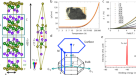
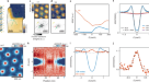
We investigate the heavy-fermion superconductor URu2Si2, which exhibits correlated narrow electron bands crossing the Fermi level and undergoes a transition to the HO phase characterized by an as yet unknown order parameter14。A partial gap opens in the electronic band structure belowTHO = 17.5 K, out of which an unconventional superconducting state develops belowTc = 1.5 K (refs. 14,18).The surface electronic states observed until now mostly have small effective masses19,20,21,22。Using STM to investigate small-sized, atomically flat terraces on the U-terminated surface of URu2Si2at sub-kelvin temperatures, we observe clearly 2DHFs with an effective mass 17 times the free electron mass, as well as quantization owing to lateral confinement and uncover the surface–bulk interaction. In Fig.1a, we present a STM image of terraces of U-terminated surfaces on URu2Si2(see Extended Data Fig.1for the surface termination). Our starting point is the tunnelling conductance obtained in a small range of a few mV around the Fermi level and at a temperature of 0.1 K, well below the superconducting critical temperature, shown in Fig.1b(see Extended Data Fig.2for a larger bias voltage range).

a, STM topography image of several U-terminated terraces on URu2Si2, cleaved perpendicular to thecaxis. The distance between terraces isc/2, that is, half a unit cell. The inset shows a zoom into the region at the white square and reveals the square U atomic surface lattice (arrows indicate the in-plane crystalline directions). The dashed rectangle represents the field of view on which we focus in Fig.2。More details about the surface termination is provided inMethodsand in Extended Data Fig.1。Scale bars, 20 nm (main), 1 nm (inset).b, Tunnelling conductance averaged along the white line ina。The dashed lines provide the features atε−,ε+and the superconducting gap discussed in theMethods。c, Height profile normalized to thec-axis lattice constant along the white line ina, indicating terracesL1toL4。d, Tunnelling conductance versus distance along the white line ina。e, Tunnelling conductance curves at different terraces. The arrows mark the positions of peaks arising from quantization due to lateral confinement. Data taken at 0.1 K.
Quantum-well states by confinement
We focus on the tunnelling conductance along the white line shown in Fig.1a。Along this line, we identify four terraces of different sizes,L1 ≈ 2 nm,L2 ≈ 5.5 nm,L3 ≈ 20 nm andL4 ≈ 38.5 nm (Fig.1c).We observe a strong bias voltage and position dependence of the tunnelling conductance, which is different for each terrace as illustrated in Fig.1d。We show in Fig.1erepresentative tunnelling conductance curves at each terrace, in which we identify a set of regular peaks.
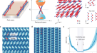
Let us analyse the terraceL3(dashed rectangle in Fig.1a).We present a symmetrized map of the tunnelling conductance in Fig.2a(seeMethodsfor further details). We identify a set of peaks in the tunnelling conductance, which evolve in both position and bias voltage. Subtracting the features atε−andε+(details provided inMethodsand in Extended Data Figs.3and4), we obtain the pattern shown in Fig.2b, which shows the lateral quantization of 2DHFs. The quantization pattern for confined electrons resembles the Fabry–Pérot expression for an interferometer made by partially reflecting mirrors23(reflection coefficientrand the phase shiftϕare the free parameters; details in Extended Data Fig.4and results on different terraces in Extended Data Fig.5).Lateral quantization results from interfering wavefunctions partially reflected at steps. Quantized levels obtained from the Fabry–Pérot expression are the white dots in Fig.2a,b, whose position coincides well with the peaks in the conductance pattern observed in the experiment. In Fig.2c, we plot as points the position of the peaks as a function of the wavevectorkand as a line the dispersion relationE = E0 + ħ2k2/ (2m*), in whichm* is the effective mass andE0the bottom of the band. We obtainE0 = −2.3 meV andm* = 17m0, withm0the free electron mass, that is, we find that the 2DHF is derived from a massive surface electron state. A detailed comparison of the tunnelling conductance versus position with the square of wavefunctions confined by a lateral potential leads to excellent fits, shown in Fig.2d。The phase shiftϕdetermines the position and energy of the peaks (white dots in Fig.2a,b) and the best account of our observations is obtained withϕ = −π. We find values aroundr ≈ 0.2, which slightly increase when approachingE0(Fig.2e).The low value ofris also found in surface states of simple metals; for example,ris between 0.2 and 0.4 in Ag and Cu (refs. 23,24,25).However, the energy dependence (Fig.2e) at the surface of URu2Si2is completely different to that in usual metals. Althoughrvaries mildly in Cu or Ag in the range of a few eV (see dashed line in Fig.2eand refs. 23,24,25), here we observe instead thatrdecreases markedly in a range of a few meV (points in Fig.2e).We can reproduce the observed dependence ofrversus bias voltage assuming a potential well23,24(continuous line in Fig.2e; details provided inMethodsand Extended Data Figs.3and4).It is also insightful to trace the tunnelling conductance as a function of the bias voltage at the centre of the terrace in Fig.2b(circles in Fig.2f) and compare it to the expectation forr ≈ 1 (dashed line in Fig.2f) and forr ≈ 0.4 (continuous line in Fig.2f).We see that, for a reducedr, both the periodicity and shape of the tunnelling conductance are well explained in an energy range of a few meV, that is, two orders of magnitude below the energy range observed in conventional metals1,2,3,4,23,24,25,26。

a, Tunnelling conductance at theL3terrace is shown by a colour scale as a function of the distance (taken at 0.1 K).b, The same data as inabut with a subtracted background (seeMethodsand Extended Data Fig.3).The white dots inaandbmark the position of peaks in the conductance. The black arrow shows the width of the quantized levels, Γ, described in the text.c, Points show the reciprocal space position of the white dots inaandb。The magenta line provides the electron dispersion relation withm* = 17m0。d, The lines show calculations and coloured points the measured tunnelling conductance.e, The dashed blue line shows the reflection coefficientrobtained in Cu(111) (seeMethods).The continuous blue line is the calculatedrassumingm* = 17m0。Points are the results obtained from the experiment.f, Tunnelling conductance as a function of the bias voltage is shown by blue circles at the centre of the terrace inb。The dashed blue line is for perfect reflection,r ≈ 1, and the continuous line forr ≈ 0.4.g, Points show the lifetime of the quantum-well states,τ, as a function of the bias voltage. The dashed blue line is the expectation for a two-dimensional electron gas and the continuous line describes quantum states whose width is set by their interaction with the heavy quasiparticles of the bulk.
To further investigate the quantized levels, we have fitted each peak to a Lorentzian function, whose width Γ (black arrow in Fig.2b) provides the lifetimeτ(Fig.2g) of the quantum-well states. Taking a two-dimensional electron gas, we expect\(\hbar /\tau ={\Gamma }_{0}+(| {E}_{0}| /4\pi ){\left[(E+| {E}_{0}| )/{E}_{0}\right]}^{2}\)\(| {\rm{ln}}| (E+| {E}_{0}| )/{E}_{0}| -{\rm{ln}}(2{q}_{{\rm{TF}}}/{k}_{{\rm{F}}})-1/2| \), withħthe reduced Planck’s constant,qTF = 0.0906 Å−1the Thomas–Fermi screening length andkFthe Fermi wavevector27(dashed line in Fig.2g).Our data are not well reproduced by this expression. Taking instead\(\hbar /\tau ={\Gamma }_{0}+(| {E}_{0}| /4\pi ){\left[(E+| {E}_{0}| )/{E}_{0}\right]}^{2}\)withE0 = −2.3 meV and Γ0 ≈ 60 μeV (continuous line in Fig.2g), we find a much better account of our data27,28。The latter expression takes into account the connection between the 2DHF and bulk states, showing that, in our experiments, the lifetimeτis set by the decay of the 2DHF into heavy-fermion bulk states. Quantum-well states sense the bulk correlations, given by the quadratic energy term inħ/τ。This has been observed in surface states of noble metals, monolayers of Pb and in Sb. However, in those cases, the energy range was three orders of magnitude above the one we discuss here3,6,11,28。
From the obtained value of Γ0 ≈ 60 μeV, we estimate the lifetime of the ground state asτ0(E0 = −2.3 meV) = ħ/Γ0 ≈ 11 ps. Similarly, the lifetime of states close to the Fermi level isτ(E = 0) = ħ/Γ(E = 0) ≈ 3 ps. We can also estimate a value for a mean free path,ℓ0 = vFħ/Γ(0) ≈ 0.14 μm, withvFthe Fermi velocity of URu2Si2。This value is on the same order of magnitude as those observed in ultraclean URu2Si2single crystals29。
To vindicate the existence of a heavy-fermion surface state, we performed density functional theory calculations of the surface band structure of a slab of URu2Si2(Extended Data Fig.6).We find a shallow, U-derived f-electron band with a flat dispersion relation compatible with our experiments around theXpoint of the simple tetragonal Brillouin zone. The bulk electronic spectrum is gapped in this part of the Brillouin zone21,22。The rest of the Brillouin zone provides surface states with much smaller effective masses.
One-dimensional edge states
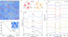
In Fig.3, we show that the 2DHF is peculiarly modified at the steps separating terraces at which one-dimensional edge states (1DESs) appear. 1DESs were previously observed in simple metals, in which a gap opens at the step and is filled with a very large density of states atE1DESby the 1DES3,8,11,24,25,30。The width of the conductance peak atE1DES,η1DES, results from inelastic scattering into bulk states24,25。Here we find that the features in the tunnelling conductance completely change at a step (Fig.3a,b).We find a high peak atE1DES ≈ −0.38 meV (Fig.3b,c) in steps, but notably only along one of the two equivalent in-plane axes, that is, an in-plane symmetry breaking occurs. The HO is known to cause breaking of the body-centred translation symmetry14, leading to inequivalent electronic properties in subsequent U layers, which is consistent with our measurements (details inMethodsand Extended Data Fig.7).This should reduce inelastic scattering and favour the formation of a 1DES. Here, however, we observe a rather unique situation in which the edge state is either observed or not, on two crystallographically equivalent in-plane axes. This indicates spontaneous symmetry breaking of the fourfold rotational symmetry close to the surface. Such in-plane symmetry breaking has been proposed31for bulk URu2Si2but has been difficult to detect. This symmetry breaking would cause an orthorhombicity given by a tiny difference in the basal-plane lattice constantsaandb(\(\frac{| \,a-b\,| }{(a+b)}\approx 1{0}^{-5}\))32。Other experiments could, however, not confirm such in-plane symmetry breaking33, which could be favoured by defects. Recent group theory considerations and nuclear magnetic resonance (NMR) data propose that the HO state can belong to four space groups, #126, #128, #134 and #136, all having the same crystal structure as the high-temperature state34。NMR experiments suggest the presence of fourfold symmetry at Ru, Si and U sites, narrowing down the most probable choice to #126 (refs. 34,35).Notably, although these measurements gave absence of fourfold symmetry breaking in bulk URu2Si2,我们的STM数据敏感个体铀ers clearly show an in-plane symmetry breaking in the 1DES. We note that a possible source of changes in the electronic structure that could also affect the 1DES is modifications of the valence of U edge atoms21。尽管如此,对称性破1 des suggests a deeper origin, which pinpoints that the 1DES serves as a sensitive probe of fundamental electronic properties of the near-surface U lattice.

a, STM image of a set of U terraces separated by steps half a unit cell in size. The colour scale provides the height, following the bar on the left. In the upper inset, we show profiles, taken along the red and blue dashed lines. The white arrows indicate the two in-plane crystal directions, which are crystallographically equivalent. The red and blue circles provide the positions at which the red and blue curves incwere taken. Scale bar, 10 nm.b, Tunnelling conductance map at the energy of the 1DES,E1DES。The colour scale is shown on the left.c, We observe the 1DES when crossing a vertical step (dashed red line ina), as shown by the tunnelling conductance versus bias voltage (red line), but not along the other in-plane crystal axis (blue line). The dashed black line is a fit and the horizontal arrow marks the width of the 1DES,η1DES(more details inMethodsand Extended Data Fig.7).
Superconductivity
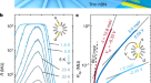
At the energy range below the superconducting gap, ΔSC ≈ 200 μeV, we observe that there is a large zero-bias conductance (see Fig.4a).There are indications for unconventional superconductivity in bulk URu2Si2, with a d-wave symmetry order parameter29。This can contribute to the suppression of the superconducting features in the tunnelling conductance, but it hardly leads to the zero-bias conductance observed in our experiment. Similar small-sized superconducting features are found in other heavy-fermion superconductors, such as CeCoIn5or UTe2, and remain difficult to explain36,37,38。Most notably, macroscopic measurements such as specific heat or thermal conductivity provide, in all these systems, a negligible zero-temperature extrapolation of the electronic density, suggesting that the superconducting density of states at the Fermi level is very small12。The 2DHF is strongly coupled to the superconducting bulk states and the proximity effect from bulk superconductivity should provide only a small amount of states at low energies. However, it is important to consider the coupling of the 2DHF to strongly energy-dependent resonant states giving peaks in the tunnelling conductance as well. The concomitant broadening then leads to a large zero-bias tunnelling conductance. Using a model that takes this into account (seeMethodsand Extended Data Fig.8), we can understand the main features of the tunnelling conductance and follow the superconducting gap with temperature (Fig.4b,c).这解决了宏观之间的差异and surface experiments and shows the relevance of two-dimensional electronic states to understanding the tunnelling conductance.

a, Tunnelling conductance versus bias voltage at zero field (red) and at 4 T (green). The fit at zero magnetic field is shown by the black line. The superconducting gap, ΔSC, is marked by an arrow.b, Tunnelling conductance versus temperature at zero field. The curves are shifted for clarity. The lines are fits to the model.c, Temperature dependence of the superconducting gap, ΔSC(T), is shown as black points. The BCS temperature dependence (line) is shown as a guide.
In summary, we have observed 2DHFs in terraced surfaces inside the HO phase of URu2Si2。The 2DHF exhibits quantum-well states with energy separation of fractions of a meV when confined between steps. The 2DHF is connected to the bulk heavy-fermion states. At steps, we observe a 1DES, which shows in-plane electronic symmetry breaking and inequivalent electronic arrangement in subsequent U layers in the HO phase. The discovery of 2DHFs and related confined states opens new possibilities to study the interplay of quantized heavy-fermion states and unconventional superconductivity, as several heavy-fermion materials show unconventional superconductivity in the bulk, often coexisting with other long-range ordered phases. Apart from URu2Si2, there are other heavy fermions, such as CeCoIn5, UBe13, UPt3or UTe2, in which the proposed superconducting states are spin-singlet d-wave or spin-triplet p-wave and f-wave states. These could exhibit 2DHFs and the associated edge states could incorporate excitations with unique properties such as Majorana fermions following non-Abelian statistics. Furthermore, because the source of quantization is lateral confinement, correlated quantum-confined states can be obtained in nanostructures built on the surface by manipulation of adatoms or by controlling layer growth in thin films15,16,39,40。This opens new avenues to generate, isolate and manipulate excitations in unconventional superconductors.
Methods
STM experiments
Single crystals of URu2Si2were grown by the Czochralski technique in a Tetra Arc Furnace. We scanned samples for a low residual resistivity and a high superconducting critical temperature, close to 1.5 K. Such samples were then cut in a bar shape with dimensions 4 × 1 × 1 mm3, with the long distance parallel to thecaxis. We mounted the samples on the sample holder of a scanning tunnelling microscope. The scanning tunnelling microscope was mounted in a dilution refrigerator. The resolution in energy of the setup was tested by measuring the superconducting tunnelling conductance with the tip and sample of s-wave superconductors Al and Pb down to 100 mK (ref. 41).Details of image-rendering software are provided in refs. 42,43。The scanning tunnelling microscope head features a low-temperature movable sample holder, which is used to cleave the sample at cryogenic temperatures41,44。At the same time, and importantly for this study, the sample holder allows modifying many times the scanning window. The terraces discussed in this work were found in three different samples, after studying hundreds of fields of view.
Surface termination in URu2Si2
We focus on U-terminated surfaces. In Extended Data Fig.1a, we show the URu2Si2crystal unit cell highlighting the U, Si and Ru planes; their inter-layer distances are indicated in units of thec-axis lattice parameter. In Extended Data Fig.1b–d, we show STM images corresponding to different surface terminations. These surfaces are all obtained after cryogenic cleaving. On the surfaces full of square-shaped terraces, we find the results obtained in the main text. An example is shown in Extended Data Fig.1b。All the observed terraces are separated byc/2 ≈ 4.84 Å. In Extended Data Fig.1c,d, we show terraces with a triangular shape, in which we do not observe the phenomena discussed in the main text. Here the distance between consecutive terraces is about 0.11c, about 0.39cor about 0.61c, which correspond, respectively, to the three possible distances between U–Si planes (coloured arrows in Extended Data Fig.1a).Therefore, we see that the surfaces with terraces having a triangular shape correspond to Si layers, sometimes with a U layer in between. By contrast, the surfaces with terraces having a square shape are U terminated. Atomically resolved images inside terraces (Extended Data Fig.1e) provide the square atomic U lattice with an in-plane constant lattice ofa = 4.12 Å . In Extended Data Fig.1f, we show a typical atomic-sized image on Si-terminated surfaces. We do not observe atomic resolution and have sometimes seen circular defects. Defects in the U-terminated surfaces are very different, as shown in Extended Data Fig.1g–o。We distinguish two distinct types of defect. The defects can be either point-like protrusions (Extended Data Fig.1g,h) or troughs (Extended Data Fig.1i).Sometimes, defects are arranged in small-sized square or rectangular structures (Extended Data Fig.1j–o).Most of these defects are probably because of vacancies or interstitial atoms in layers below the U surface layer.
Tunnelling conductance in the HO state
The tunnelling conductance of the HO state has been discussed in refs. 45,46,47,48,49。We have reproduced the results, as shown in Extended Data Fig.2a,b。The tunnelling conductance results from simultaneous tunnelling into heavy and light bands, as in other heavy-fermion compounds50,51,52。The red line in Extended Data Fig.2aforT = 18 K follows a Fano function
in whichAis a constant of proportionality,qis the ratio between two tunnelling paths andEFanois the Fano resonance energy with width\({\Gamma }_{{\rm{F}}}=2\sqrt{{(\pi {k}_{{\rm{B}}}T)}^{2}+2{({k}_{{\rm{B}}}{T}_{{\rm{K}}})}^{2}}\),TKbeing the Kondo temperature45,46。For the fit, we include an asymmetric linear background owing to the degree of particle–hole asymmetry in the light conduction band45,53。To account for the thermal broadening, we convolute the result with the derivative of the Fermi–Dirac distribution. We findq = 0.8 ± 0.5,EFano = 3 ± 1 mV, ΓF = 22 ± 1 mV andTK = 90 ± 5 K, consistent with previous reports45,46。
Inside the HO phase (red line in Extended Data Fig.2b), we use the same Fano function, multiplied by an asymmetric BCS-like gap function with an offsetδE
The resulting function is convoluted with the derivative of the Fermi–Dirac distribution function. We findδE(4.1 K) = 1.5 ± 0.5 meV and ΔHO(4.1 K) = 4.0 ± 0.5 meV, consistent with previous reports45,46。
Note that we also observe further features at lower temperatures and smaller bias voltages (Extended Data Fig.2c).The red line in Extended Data Fig.2cis a fit described below. The features above the superconducting gap can also be roughly obtained by using two Lorentzians atε−andε+and an asymmetric background. Probably, the peaks atε−andε+are because of avoided crossings in the band structure of the 2DHF at very low energies. We notice that the small feature atε+occurs at a very similar energy range as a kink in the band structure found at the surface of Th-doped URu2Si2(refs. 48,49).In the calculations we show below, we can identify features in surface f-derived bands that can be associated to such peaks in the tunnelling conductance. However, such features can form as a result of correlations elsewhere in the Brillouin zone as well.
Quantum-well states at terraces between steps
In Extended Data Fig.3a, we show the tunnelling conductance background subtracted from Fig.2ato obtain Fig.2b。To carry out the background subtraction, we first identify the features atε−andε+in the conductance map. These are the light-blue regions centred atε+and the red–yellow region centred atε−in Extended Data Fig.3a。We then identify the edge states occurring at the steps, given by the red areas at the sides of Extended Data Fig.3a。Similar peaks are obtained on steps separating different terraces. The nature and shape of the 1DESs is discussed below. We then model these features by a set of Lorentzians and obtain the pattern shown in Extended Data Fig.3a。We subtract this pattern from the experiment (Fig.2a) to obtain the pattern shown in Extended Data Fig.3b。
To model the quantum-well states, we use the Fabry–Pérot interferometer expression for the density of statesgFP(x, E) given by
with\(k=\sqrt{2{m}^{* }(E-{E}_{0})/{\hbar }^{2}}\),m* the electronic effective mass,rthe reflection amplitude,ϕthe phase andLthe width of the terrace23。法布里-珀罗干涉仪是一种光学resonator made of semireflecting mirrors and provides a simple and insightful way to model electronic wavefunctions confined between two wells. More information on surface band structure and on quantum-well states by confinement is provided in refs. 3,9,54,55,56,57,58,59,60。We assume a symmetric potential well withL = 20 nm,r = 0.5 andϕ = −π. The pattern generated by equation (3) is shown in Extended Data Fig.3c。White points provide the positions of quantized levels as in Fig.2a,b。It is not difficult to see that the structure of quantized levels is renormalized together with the electronic band structure. Smaller electronic effective masses imply larger quantized level width and separation, and vice versa. However, the simple Fabry–Pérot model does not take into account relaxation by electron–electron interactions, which lead to the extra level broadening discussed in the main text and in refs. 27,28,61。
The black lines in Fig.2dare fits to the equation (3).To account for the behaviour at the edges, we add the equation (5) for the 1DES. We use the parameters extracted for the terraceL3, discussed in Extended Data Table1。We show further examples in Extended Data Fig.4。Note that, in Fig.2d, we use equation (3) along with the contribution from the 1DES and contributions forε−andε+at the bias voltages at which these features are observed in the tunnelling conductance.
The 2DHF quantization was observed on the surfaces of different URu2Si2samples. In Extended Data Fig.5a–c, we show the result on another sample. Notice here that terraces have different sizes. We show in Extended Data Fig.5athe STM topography image. In Extended Data Fig.5b, we show a height profile through the white line in Extended Data Fig.5a。In Extended Data Fig.5c, we represent the tunnelling conductance along the central terrace (L ≈ 57 nm) of this profile. We observe similar tunnelling conductance curves as those presented in the main text. Notice the features atε−andε+。The quantized levels are also readily observed. These occur, however, at different energy values, as the size of the terraceLis different to that of the terrace in the main text. In Extended Data Fig.5d, we represent the values of the quantized levels found in terraces of different sizesLby different colours; we show the dispersion relation of the 2DHF as a magenta line.
In Extended Data Fig.5e, we show as coloured points the bias voltage dependence of the energy spacing ΔE连续量子化的l之间evels for terracesL3,L4, the terrace with lengthL = 57 nm (shown in Extended Data Fig.5c) and a terrace with lengthL = 27 nm (not shown). We can write that\(\Delta E={E}_{n+1}-{E}_{n}=\left(\frac{{\hbar }^{2}{\pi }^{2}}{2{m}^{* }{L}^{2}}\right)\left({(n+1)}^{2}-{n}^{2}\right)\), withn = 1, 2, 3,…. This gives a square-root dependence of ΔEon the energy,\(\Delta E={E}_{n+1}-{E}_{n}=\left(\frac{{\hbar }^{2}{\pi }^{2}}{2{m}^{* }{L}^{2}}\right)\left(2n+1\right)\propto \sqrt{E}\), shown in Extended Data Fig.5e。In Extended Data Fig.5f, we plot the average value of\(\frac{\Delta E}{2n+1}\)for each terrace as a function ofL。We find the expected\(\frac{1}{{L}^{2}}\)dependence.
Note that in Extended Data Fig.5and Fig.1d, we do not perform any symmetrization. We can see a tendency of the quantized states to shift towards the sides of the terrace, giving intensity patterns that are slightly asymmetric. We have calculated the expected patterns for different reflection coefficients at each side of the terrace. This produces asymmetric patterns similar to those observed experimentally. However, it is difficult to separate such an asymmetry from the signal coming from the edge states in the tunnelling conductance. Lateral symmetrization thus remains the best way to analyse and understand quantum states in the terraces observed here in URu2Si2。
We use\(\hbar /\tau ={\Gamma }_{0}+\left(| {E}_{0}| /4\pi \right){\left[(E+| {E}_{0}| )/{E}_{0}\right]}^{2}\)to fit the energy dependence of the lifetime61。The parameter |E0|/4π is a prefactor that fits our experiment well. The prefactor is sometimes provided as a number28and has also been estimated as\(\frac{{e}^{2}{k}_{{\rm{F}}}^{2}\pi }{4\pi {{\epsilon }}_{0}\,32\,\hbar {q}_{{\rm{TF}}}}\)or, equivalently,\(\frac{e{m}^{3/2}}{32\times {3}^{5/6}{\pi }^{2/3}{{\epsilon }}_{0}^{1/2}{\hbar }^{4}{n}^{5/6}}\)(withϵ0the dielectric constant,nthe electron density andqTFthe Thomas–Fermi screening length)27。These estimations provide similar values to |E0|/4π.
To obtain the energy dependence of the reflection coefficient,r(E), we used the model described in ref. 24。To this end, we consider a one-dimensional periodic array of scattering objects, each modelled by a square potential well of widthb < L(Lis the width of the terrace). A constant complex potentialWprovides confinement and coupling to the bulk states. We can then write
with\(k=\sqrt{\frac{2{m}^{* }E}{{\hbar }^{2}}}\)and\(q=\sqrt{\frac{2{m}^{* }(E-W)}{{\hbar }^{2}}}\)。The reflection coefficientr(E) is given byr(E) = |R(E)|2。For the dashed line in Fig.2e, we use typical parameters for Cu, withm* = 0.46m0andW = (−2 − 1i) eV. We shift the obtained curve in energy to obtain a result within the energy range of our data. For the continuous line in Fig.2e, we usem* = 17m0andW = (−18 − 5i) meV.
Band-structure calculations at U-terminated surfaces of URu2Si2
The band structure of bulk URu2Si2has been analysed previously in detail using DFT calculations62,63,64。Relevant results coincide with angle-resolved photoemission, STM and quantum oscillation studies22,65,66,67,68,69,70,71。
Several surface states have been observed by angle-resolved photoemission spectroscopy19,20,21,22。The surface state discussed in refs. 19,20is formed by a hole-like band with its maximum at −35 meV and is thus far from what we observe here. At theXpoint of the Brillouin zone, there are no bulk states. Angle-resolved photoemission spectroscopy measurements show hints of surface-like bands with two-dimensional character at these points21。We have taken a closer look at theXpoint through DFT calculations. To this end, we built a U-terminated supercell consisting of 37 atomic layers, giving a total of ten U layers (Extended Data Fig.6a).We performed DFT calculations using the full-potential linearized augmented plane-wave method with local orbitals as implemented in the WIEN2k package72。Atomic spheres radii were set to 2.5, 2.5 and 1.9 Bohr radii for U, Ru and Si, respectively. We used a 19 × 19 × 1 mesh ofk-points in the first Brillouin zone, reduced by symmetry to 55 distinctk-points. The RKmaxparameter was set to 6.5, resulting in a basis size of approximately 5,400 (more than 100 basis functions per atom). Spin–orbital coupling was included in the second variational step73和当地轨道包括了相对论U 6p1/2and Ru 4p1/2states. The basis for calculations of the spin–orbital eigenvalue problem consisted of scalar-relativistic valence states of energies up to about 5 Ry, resulting in a basis size of about 3,800. The local density approximation was used for the treatment of exchange and correlation effects63,74。
In Extended Data Fig.6b, we highlight in particular the U spin-up character of the obtained surface-projected band structure. The spin-down character is much less pronounced within the shown energy range. There are several bands inside gaps of the bulk band structure, but only those around theXpoint of the simple tetragonal Brillouin zone,Xst(see Extended Data Fig.6c), are sufficiently shallow to provide large effective masses.
We find a surface state (upper inset of Extended Data Fig.6b),包括两个杂交孔乐队,形式ing an M-shaped feature close to the Fermi level. The dispersion relation found in our experiment (magenta line in the upper inset of Extended Data Fig.6b) is compatible with the central part of the M-shaped feature.
1DES and HO within U layers
To analyse the 1DES at the step between two terraces, we use a one-dimensional Dirac-function-like potential at the step,V(x) = U0δ(x − x1DES), in whichx1DESis the position of the 1DES. We takeU0 = b0V0, withb0the width of the potential well andV0the energy depth (V0 < 0). We add a complex potential,V(x)→(U0 − iU1)δ(x − x1DES) to simulate the coupling of the 1DES to the bulk of the crystal. A schematic representation of this model is shown in Extended Data Fig.7a。Solving the Schrödinger equation forE < 0, we obtain the Green’s function of the states in the potential well
in which\({\lambda }_{x}=\frac{{\hbar }^{2}}{{m}^{* }}| {U}_{0}{| }^{-1}\)is the decay length withm* the effective mass.E1DESandη1DESare the energy position and the energy broadening of the 1DES given by
in whichδVis the height of the potential barrier of the well relative to the Fermi level.
We can now fit the tunnelling conductance at the 1DES using
convoluted with the derivative of the Fermi–Dirac distribution function. Extended Data Table1shows the extracted fitting parametersE1DES,η1DES,λxandx1DESfor the four different terracesL1toL4from Fig.1。
From Extended Data Table1, we see that the energy position and the energy broadening of the 1DES are independent of the terrace size, with average values ofE1DES = −0.52 ± 0.14 meV andη1DES = 0.45 ± 0.06 meV. We also see that all the spatial features are always at the same position with respect to the step,x1DES ≈ 4.0a0,a0being the in-plane lattice constant, with a decay lengthλx ≈ 0.9 nm ≈ 2a0。The latter indicates that 1DESs and 2DHFs couple when the decay length reaches a few interatomic distances. With the extracted average values from Extended Data Table1forλx,η1DESandE1DES, we obtainU0 = 5.4 meVÅ,U1 = 0.38 meVÅ andδV = 3.1 meV.
We can analyse the 1DES through the tunnelling conductance at a step (Extended Data Fig.7b,c).At low bias voltages, we find a dip in the tunnelling conductance of a few nanometres at the upper side of the step (blue lines in Extended Data Fig.7b; for example, at −1.2 mV). The dip fills with the 1DES at aboutE1DES(red lines in Extended Data Fig.7bat −0.4 mV) and empties again at higher bias voltages. This shows that charge depletion close to the step opens a gap in the band structure. The gap is filled at the resonant energy of the 1DES, as observed previously in metals30,75,76。By normalizing the tunnelling conductance to its shape far from the step (Extended Data Fig.7c), we can follow the decay of the 1DES into the quantum-well states of the 2DHF with the model described above (Extended Data Fig.7a).The decay length is on the order of the inverse of the wavevector of the 2DHF.
Taking a closer look at the steps, we surprisingly find a notable in-plane anisotropy of the 1DES. As we see in Extended Data Fig.7b, the 1DES is observed when crossing steps along the dashed red line in Extended Data Fig.7bbut not along the dashed blue line, as discussed in the main text. It is useful here to take a closer look at the HO as well. As discussed in refs. 14,34,64,77,78,79, there is no dipolar (magnetic) or structural order related to the HO phase. Instead, the U lattice can present some sort of long-range electronic ordering, whose actual symmetry and shape is considered as a relevant and open mystery14。
Previous NMR measurements indicated the absence of fourfold in-plane symmetry breaking in bulk URu2Si2(ref. 35), whereas our STM data clearly show an in-plane symmetry breaking in the 1DES. At the surface, there can be marked changes in the electronic structure owing to a modification of the valence of uranium atoms21,80。Rather, the breaking of the in-plane symmetry observed here in the 1DES suggests that a fundamental breaking of the near-surface electronic properties of the U lattice is at play in the HO phase.
Interplay between superconductivity and the 2DHF
We consider several parallel conduction channels between the tip and the surface. For simplicity, we take into account tunnelling into the 2DHF and into the feature of largest size atε−(Extended Data Fig.8a).The first channel,t1, connects the tip with the 2DHF. The 2DHF is superconducting by proximity from the bulk superconductor, which we model using a couplingts。With the second channel,t2, we connect the tip to other surface features. We can write the retarded Green function\({\hat{G}}^{{\rm{r}}}\)as
with
in whichE2DHFis the energy associated to the 2DHF and includes the shift of energy owing to HO and Fano resonance,Wis an energy scale related to the normal density of states at the Fermi level byρ(EF) = 1/(πW), Δ is the superconducting gap andηis a small energy relaxation rate. We have added the self energiesiΓj/2, (j = 2DHF, −, +), with Γjthe width of the resonancej。
The differential conductance is calculated as
with
Heref(E, T) is the Fermi–Dirac distribution at the energyEand temperatureTand\({\sigma }_{0}=\frac{2{e}^{2}}{h}\)is the quantum of conductance (withhbeing Planck’s constant andethe elementary charge). Notice thatTis the transmission, not the density of states often used to discuss STM measurements in superconductors. Notice also that we take into account tunnelling into the 2DHF (\({G}_{11}^{{\rm{r}}}\)) and intoε−(\({G}_{33}^{{\rm{r}}}\)), with mixed contributions (\({G}_{31}^{{\rm{r}}}\)and\({G}_{13}^{{\rm{r}}}\)).
To fit the tunnelling conductance curves shown in Fig.4a,band Extended Data Fig.8b, we subtracted an asymmetric background (see Extended Data Figs.2and8b).In Extended Data Table2, we show the parameters used to obtain the tunnelling conductance with temperature (shown as black lines in Fig.4a,b) from equation (11).We do not vary the parametersη = 0.018 meV,ε2DHF = 12 meV, Γ2DHF = 1 meV, Γ− = 0.55 meV and Γ+ = 0.14 meV with temperature. We see that the superconducting lifetime itself is practically negligible,η = 0.018 meV ≪ Δ = 0.2 meV. The large zero-bias conductance is not because of the incomplete coupling to the bulk, astsis close to one. There is further smearing coming from features atε+andε−。Γ+and Γ−provide the smeared superconducting density of states and a finite tunnelling conductance at zero bias. Notice that the superconducting gap vanishes at the critical temperatureTcbut that the strongly bias-voltage-dependent tunnelling conductance remains up to higher temperatures (Extended Data Fig.8).
There are numerous evidences for d-wave or more complex superconducting properties in URu2Si2。超导密度的差异f states between these superconducting states and s-wave superconductivity are relatively small, particularly because the tunnelling conductance obtained with the model described here provides smeared conductance curves. The same occurs for the temperature dependence of the superconducting gap. Instead, the shape and asymmetry of the tunnelling conductance at defects might provide the connection between the properties of the superconducting 2DHF and the unconventional superconductivity of the bulk.
Results at point defects
We analyse in more detail here the tunnelling conductance at defects. We plot the tunnelling conductance obtained on two different defects in Extended Data Fig.9aas blue and red lines. Notice the pronounced electron–hole asymmetry, which provides curves that widely differ from the curves far from defects (black line in Extended Data Fig.9a).As discussed above, we can identify two kinds of defects: protrusions with height increases of around 15 pm, probably because of interstitial atoms located beneath the surface (Extended Data Fig.9b,d,f,h的下午15点左右),波谷大小,可能because of vacancies beneath the surface (Extended Data Fig.9c,e,g,i).The defects visibly affect the tunnelling conductance. We plot the tunnelling conductance atε+, 0 mV andε−for both types of defect in Extended Data Fig.9f,g。In Extended Data Fig.9h,i, we show the spatial dependence of the tunnelling conductance along a crystalline axis for both types of defect. At the site of the defect, there is a pronounced electron–hole asymmetry, which is opposite for each kind of defect. Protrusions provide a substantially enhanced tunnelling conductance for empty states above the Fermi level, whereas troughs provide the opposite (Extended Data Fig.9a).At zero bias, the troughs show a pronounced in-plane anisotropy and a reduction of the superconducting gap, whereas the protrusions are in-plane isotropic and show an opened superconducting gap. When leaving the defect, the usual behaviour is recovered after several nanometres (Extended Data Fig.9h,i).
To explain the pronounced modification of the electron–hole asymmetry of the tunnelling conductance, let us consider electron correlations creating a large Fermi surface scenario at some portion of the band structure. At low temperatures, correlations provide an avoided band crossing owing to hybridized heavy and light bands. We can assume that it happens somewhere in the band structure of URu2Si2, for example, close to the Γ point, as suggested in refs. 14,18,47。Then, we obtain at low temperatures a large Fermi surface with heavy electrons and a close-lying light band with smaller wavevectors above the Fermi level. We can then assume that both kinds of defect couple to different parts of such a correlated band structure. Following our experiments, protrusions create 2DHF coupling to the small light band and a large density of states for empty states above the Fermi level (red curve in Extended Data Fig.9a).Troughs can instead favour coupling to the heavy band, giving the opposite behaviour (blue curve in Extended Data Fig.9a).The superconducting gap is disturbed at troughs. Generally, we expect all sorts of defects to be pair breaking, as URu2Si2is not a s-wave superconductor. However, two-dimensional quantized states screen pair-breaking interactions from the underlying superconducting bulk81。This suggests that the absence of in-gap states in protrusions is because of screening by the 2DHF. Troughs, however, produce a strong coupling to the heavy bands that carry the heavy superconducting state and thus also contribute to pair breaking.
In-gap states at troughs have a certain in-plane anisotropy (Extended Data Fig.9g, middle panel). The anisotropy of the superconducting gap has been analysed with macroscopic measurements82,83,84,85。There are indications for gap nodes, for instance, from specific heat measurements82,83,85。Local vortex dynamics shows an in-plane fourfold or twofold pinning potential86。When measured as a function of the angle, there is a pronounced out-of-plane anisotropy, which has been associated to nodes along thecaxis, but there is little in-plane variation85。Following such a nodal structure, several experiments propose a chiralkz(kx + iky) superconducting wavefunction84,85,87。The surface states of a (kx ± iky) superconductor are predicted to be chiral arc states connecting the Weyl nodes88。,目前还不清楚这些表面的状态the superconducting phase adapt to the surface states of the normal phase, which appear as a consequence of the surface-induced perturbation of the crystalline potential. As mentioned, we observe an asymmetry at zero bias (Extended Data Fig.9g, middle panel). To increase the signal-to-noise ratio, we were forced to apply a fourfold symmetrization. Thus, the anisotropy might be twofold or fourfold. The chiralkz(kx + iky) state is in-plane isotropic. However, the shape of in-gap states is determined by the anisotropy of the normal-state wavefunctions, together with the symmetry of the superconducting wavefunction, so that the observed in-plane anisotropy of the in-gap states probably reflects the normal-state in-plane anisotropy.
Data availability
All data supporting the findings of this study are available from the corresponding authors on request.
Code availability
The simulation code WIEN2k used to compute the surface electronic band structure can be obtained fromhttp://susi.theochem.tuwien.ac.at。
References
Hasegawa, Y. & Avouris, P. Direct observation of standing wave formation at surface steps using scanning tunneling spectroscopy.理论物理。Rev. Lett.71, 1071–1074 (1993).
Crommie, M. F., Lutz, C. P. & Eigler, D. M. Imaging standing waves in a two-dimensional electron gas.Nature363, 524–527 (1993).
Echenique, P. & Pendry, J. Theory of image states at metal surfaces.Prog. Surf. Sci.32, 111–159 (1989).
Li, J., Schneider, W.-D., Berndt, R. & Crampin, S. Electron confinement to nanoscale Ag islands on Ag(111): a quantitative study.理论物理。Rev. Lett.80, 3332–3335 (1998).
Wenderoth, M. et al. Low-temperature scanning tunneling spectroscopy as a probe for a confined electron gas.Europhys. Lett.45, 579–584 (1999).
Bürgi, L., Jeandupeux, O., Brune, H. & Kern, K. Probing hot-electron dynamics at surfaces with a cold scanning tunneling microscope.理论物理。Rev. Lett.82, 4516–4519 (1999).
Crommie, M. F., Lutz, C. P. & Eigler, D. M. Confinement of electrons to quantum corrals on a metal surface.Science262, 218–220 (1993).
Heller, E. J., Crommie, M. F., Lutz, C. P. & Eigler, D. M. Scattering and absorption of surface electron waves in quantum corrals.Nature369, 464–466 (1994).
Fiete, G. A. & Heller, E. J. Colloquium: Theory of quantum corrals and quantum mirages.Rev. Mod. Phys.75, 933–948 (2003).
Manoharan, H. C., Lutz, C. P. & Eigler, D. M. Quantum mirages formed by coherent projection of electronic structure.Nature403, 512–515 (2000).
Kirchmann, P. S. et al. Quasiparticle lifetimes in metallic quantum-well nanostructures.Nat. Phys.6, 782–785 (2010).
Hewson, A. C.The Kondo Problem to Heavy Fermions(Cambridge Univ. Press, 1993).
Patil, S. et al. ARPES view on surface and bulk hybridization phenomena in the antiferromagnetic Kondo lattice CeRh2Si2。Nat. Commun.7, 11029 (2016).
Mydosh, J. A. & Oppeneer, P. M. Hidden order behaviour in URu2Si2(a critical review of the status of hidden order in 2014).Philos. Mag.94, 3642–3662 (2014).
Shishido, H. et al. Tuning the dimensionality of the heavy fermion compound CeIn3。Science327, 980–983 (2010).
Mizukami, H. et al. Extremely strong-coupling superconductivity in artificial two-dimensional Kondo lattices.Nat. Phys.7, 849–853 (2011).
Pirie, H. et al. Imaging emergent heavy Dirac fermions of a topological Kondo insulator.Nat. Phys.16, 52–56 (2020).
Oppeneer, P. M. et al. Spin and orbital hybridization at specifically nested Fermi surfaces in URu2Si2。理论物理。启B84, 241102 (2011).
Boariu, F. et al. The surface state of URu2Si2。J. Electron Spectrosc. Relat. Phenom.181, 82–87 (2010).
Zhang, W. et al. ARPES/STM study of the surface terminations and 5f-electron character in URu2Si2。理论物理。启B98, 115121 (2018).
Fujimori, S.-I., Takeda, Y., Yamagami, H., Yamamoto, E. & Haga, Y. Electronic structure of URu2Si2in paramagnetic phase: three-dimensional angle resolved photoelectron spectroscopy study.Electron. Struct.3, 024008 (2021).
Denlinger, J. D. et al. Global perspectives of the bulk electronic structure of URu2Si2from angle-resolved photoemission.Electron. Struct.4, 013001 (2022).
Bürgi, L., Jeandupeux, O., Hirstein, A., Brune, H. & Kern, K. Confinement of surface state electrons in Fabry-Pérot resonators.理论物理。Rev. Lett.81, 5370–5373 (1998).
Hörmandinger, G. & Pendry, J. B. Interaction of surface states with rows of adsorbed atoms and other one-dimensional scatterers.理论物理。启B50, 18607–18620 (1994).
Crampin, S., Boon, M. H. & Inglesfield, J. E. Influence of bulk states on laterally confined surface state electrons.理论物理。Rev. Lett.73, 1015–1018 (1994).
Gartland, P. O. & Slagsvold, B. J. Transitions conserving parallel momentum in photoemission from the (111) face of copper.理论物理。启B12, 4047–4058 (1975).
Giuliani, G. F. & Quinn, J. J. Lifetime of a quasiparticle in a two-dimensional electron gas.理论物理。启B26, 4421–4428 (1982).
Seo, J. et al. Transmission of topological surface states through surface barriers.Nature466, 343–346 (2010).
Kasahara, Y. et al. Superconducting gap structure of heavy-fermion compound URu2Si2determined by angle-resolved thermal conductivity.New J. Phys.11, 055061 (2009).
Ortega, J. E., Himpsel, F. J., Haight, R. & Peale, D. R. One-dimensional image state on stepped Cu(100).理论物理。启B49, 13859 (1994).
Okazaki, R. et al. Rotational symmetry breaking in the hidden-order phase of URu2Si2。Science331, 439–442 (2011).
Tonegawa, S. et al. Direct observation of lattice symmetry breaking at the hidden-order transition in URu2Si2。Nat. Commun.5, 5188 (2014).
Choi, J. et al. Pressure-induced rotational symmetry breaking in URu2Si2。理论物理。启B98, 241113 (2018).
Harima, H. Hidden-orders of uranium compounds.SciPost, scipost_202208_00031v1 (2022).
Kambe, S. et al. Odd-parity electronic multipolar ordering in URu2Si2: conclusions from Si and Ru NMR measurements.理论物理。启B97, 235142 (2018).
Allan, M. P. et al. Imaging Cooper pairing of heavy fermions in CeCoIn5。Nat. Phys.9, 468–473 (2013).
Zhou, B. B. et al. Visualizing nodal heavy fermion superconductivity in CeCoIn5。Nat. Phys.9, 474–479 (2013).
Jiao, L. et al. Chiral superconductivity in heavy-fermion metal UTe2。Nature579, 523–527 (2020).
Chatterjee, S. Heavy fermion thin films: progress and prospects.Electron. Struct.3, 043001 (2021).
Jourdan, M., Huth, M. & Adrian, H. Superconductivity mediated by spin fluctuations in the heavy-fermion compound UPd2Al3。Nature398, 47–49 (1999).
Fernández-Lomana, M. et al. Millikelvin scanning tunneling microscope at 20/22 T with a graphite enabled stick-slip approach and an energy resolution below 8 μeV: application to conductance quantization at 20 T in single atom point contacts of Al and Au and to the charge density wave of 2H-NbSe2。Rev. Sci. Instrum.92, 093701 (2021).
Martín-Vega, F. et al. Simplified feedback control system for scanning tunneling microscopy.Rev. Sci. Instrum.92, 103705 (2021).
Horcas, I. et al. WSXM: a software for scanning probe microscopy and a tool for nanotechnology.Rev. Sci. Instrum.78, 013705 (2007).
Suderow, H., Guillamon, I. & Vieira, S. Compact very low temperature scanning tunneling microscope with mechanically driven horizontal linear positioning stage.Rev. Sci. Instrum.82, 033711 (2011).
Schmidt, A. R. et al. Imaging the Fano lattice to hidden order transition in URu2Si2。Nature465, 570–576 (2010).
Aynajian, P. et al. Visualizing the formation of the Kondo lattice and the hidden order in URu2Si2。Proc. Natl Acad. Sci.107, 10383–10388 (2010).
Yuan, T., Figgins, J. & Morr, D. K. Hidden order transition in URu2Si2: evidence for the emergence of a coherent Anderson lattice from scanning tunneling spectroscopy.理论物理。启B86, 035129 (2012).
Hamidian, M. H. et al. How Kondo-holes create intense nanoscale heavy-fermion hybridization disorder.Proc. Natl Acad. Sci.108, 18233–18237 (2011).
Morr, D. K. Theory of scanning tunneling spectroscopy: from Kondo impurities to heavy fermion materials.Rep. Prog. Phys.80, 014502 (2016).
Löhneysen, H. V., Rosch, A., Vojta, M. & Wölfle, P. Fermi-liquid instabilities at magnetic quantum phase transitions.Rev. Mod. Phys.79, 1015–1075 (2007).
Coleman, P.Heavy Fermions: Electrons at the Edge of Magnetism, Chs. 1–3, 1–217 (Wiley, 2007).
Flouquet, J. inProgress in Low Temperature PhysicsVol. 15 (ed. Halperin, W. P.) 139–281 (Elsevier, 2005).
Figgins, J. & Morr, D. K. Differential conductance and quantum interference in Kondo systems.理论物理。Rev. Lett.104, 187202 (2010).
Fu, Y.-S. et al. Manipulating the Kondo resonance through quantum size effects.理论物理。Rev. Lett.99, 256601 (2007).
Crommie, M. F., Lutz, C. P., Eigler, D. M. & Heller, E. J. Quantum corrals.理论物理。D Nonlinear Phenom.83, 98–108 (1995).
Crommie, M. F., Lutz, C. P., Eigler, D. M. & Heller, E. J. Quantum interference in 2D atomic-scale structures.Surf. Sci.361, 864–869 (1996).
Tamm, I. Über eine mögliche Art der Elektronenbindung an Kristalloberflächen.Z. Phys.76, 849–850 (1932).
Shockley, W. On the surface states associated with a periodic potential.理论物理。Rev.56, 317–323 (1939).
Kevan, S. & Eberhardt, W. in Kevan, S. (ed.)Angle-Resolved Photoemission: Theory and Current ApplicationsVol. 74 (ed. Kevan, S.) 99–143 (Elsevier, 1992).
Fiete, g . a . et al。近藤米尔的散射理论ages and observation of single Kondo atom phase shift.理论物理。Rev. Lett.86, 2392–2395 (2001).
Giuliani, G. & Vignale, G.Quantum Theory of the Electron Liquid(Cambridge Univ. Press, 2005).
Oppeneer, P. M. et al. Electronic structure theory of the hidden-order material URu2Si2。理论物理。启B82, 205103 (2010).
Elgazzar, S., Rusz, J., Amft, M., Oppeneer, P. M. & Mydosh, J. A. Hidden order in URu2Si2originates from Fermi surface gapping induced by dynamic symmetry breaking.Nat. Mater.8, 337–341 (2009).
Ikeda, H. et al. Emergent rank-5 nematic order in URu2Si2。Nat. Phys.8, 528–533 (2012).
Aoki, D. et al. High-field Fermi surface properties in the low-carrier heavy-fermion compound URu2Si2。J. Phys. Soc. Jpn.81, 074715 (2012).
Onuki, H. et al. Fermi surface properties and de Haas–van Alphen oscillation in both the normal and superconducting mixed states of URu2Si2。Philos. Mag. B79, 1045–1077 (1999).
Yoshida, R. et al. Signature of hidden order and evidence for periodicity modification in URu2Si2。理论物理。启B82, 205108 (2010).
Kawasaki, I. et al. Electronic structure of URu2Si2in paramagnetic phase studied by soft x-ray photoemission spectroscopy.J. Phys. Conf. Ser.273, 012039 (2011).
孟,J.-Q。et al。成像the three dimensional Fermi surface pairing near the hidden order transition in URu2Si2using angle-resolved photoemission spectroscopy.理论物理。Rev. Lett.111, 127002 (2013).
Bareille, C. et al. Momentum-resolved hidden-order gap reveals symmetry breaking and origin of entropy loss in URu2Si2。Nat. Commun.5, 4326 (2014).
Santander-Syro, A. F. et al. Fermi-surface instability at the ‘hidden-order’ transition of URu2Si2。Nat. Phys.5, 637–641 (2009).
Blaha, P. et al. WIEN2k: an APW+lo program for calculating the properties of solids.J. Chem. Phys.152, 074101 (2020).
Kuneš, J., Novák, P., Diviš, M. & Oppeneer, P. M. Magnetic, magneto-optical, and structural properties of URhAl from first-principles calculations.理论物理。启B63, 205111 (2001).
Perdew, J. P. & Wang, Y. Accurate and simple analytic representation of the electron-gas correlation energy.理论物理。启B45, 13244–13249 (1992).
Namba, H., Nakanishi, N., Yamaguchi, T. & Kuroda, H. Electronic states localized at step edges on Ni(7 9 11) surfaces studied by angle-resolved photoelectron spectroscopy.理论物理。Rev. Lett.71, 4027–4030 (1993).
Avouris, P. & Lyo, I.-W. Observation of quantum-size effects at room temperature on metal surfaces with STM.Science264, 942–945 (1994).
Chandra, P., Coleman, P. & Flint, R. Hastatic order in the heavy-fermion compound URu2Si2。Nature493, 621–626 (2013).
Broholm, C. L. et al. Strict limit on in-plane ordered magnetic dipole moment in URu2Si2。理论物理。启B89, 155122 (2014).
Harima, H., Miyake, K. & Flouquet, J. Why the hidden order in URu2Si2is still hidden—one simple answer.J. Phys. Soc. Jpn.79, 033705 (2010).
Johansson, B. Valence state at the surface of rare-earth metals.理论物理。启B71, 6615 (1979).
Morr, D. K. & Stavropoulos, N. A. Quantum corrals, eigenmodes, and quantum mirages ins-wave superconductors.理论物理。Rev. Lett.92, 107006 (2004).
Fisher, R. A. et al. Specific heat of URu2Si2: effect of pressure and magnetic field on the magnetic and superconducting transitions.理论物理。B Condens. Matter163, 419–423 (1990).
Brison, J. P. et al. Very low temperature properties of heavy fermion materials.理论物理。B Condens. Matter199, 70–75 (1994).
Kasahara, Y. et al. Superconducting gap structure of heavy-Fermion compound URu2Si2determined by angle-resolved thermal conductivity.New J. Phys.11, 055061 (2009).
Yano, K. et al. Field-angle-dependent specific heat measurements and gap determination of a heavy fermion superconductor URu2Si2。理论物理。Rev. Lett.100, 017004 (2008).
Iguchi, Y. et al. Local observation of linear-Tsuperfluid density and anomalous vortex dynamics in URu2Si2。理论物理。启B103, L220503 (2021).
Kittaka, S. et al. Evidence for chirald-wave superconductivity in URu2Si2from the field-angle variation of its specific heat.J. Phys. Soc. Jpn.85, 033704 (2016).
Schnyder, A. P. & Brydon, P. M. R. Topological surface states in nodal superconductors.J. Phys. Condens. Matter27, 243201 (2015).
Acknowledgements
我们承认讨论w HO的对称ith H. Harima. This work was supported by the Spanish State Research Agency (PID2020-114071RB-I00, PID2020-117671GB-I00 and CEX2018-000805-M), by the Comunidad de Madrid through the programme NanomagCOST-CM (programme no. S2018/NMT-4321) and by EU (PNICTEYES ERC-StG-679080 and COST SUPERQUMAP CA21144). H.S., E.H. and I.G. acknowledge SEGAINVEX at UAM for the design and construction of the STM cryogenic equipment. J.A.G. and E.H. acknowledge the support of the Ministerio de Ciencia, Tecnología e Innovación de Colombia (grants 122585271058 and 784(2017)). W.J.H. and E.H. acknowledge support from the Universidad Nacional de Colombia (DIEB projects 48148, 57522 and 201010025979(2016)). J.P.B. and G.K. acknowledge support from the French National Agency for Research (ANR) within the projects FRESCO no. ANR-20-CE30-0020 and FETTOM ANR-19-CE30-0037. J.R. and P.M.O. acknowledge support from the Swedish Research Council (VR), the Knut and Alice Wallenberg Foundation (grant no. 2022.0079) and the Swedish National Infrastructure for Computing (SNIC), through grant no. 2018-05973.
Author information
Authors and Affiliations
Contributions
E.H. performed the study and made all experiments, with the supervision of I.G. E.H. analysed the data and compared with theory, with the supervision of W.H. and J.A.G. J.R. and P.M.O. performed the band-structure calculations and discussed the features of surface states. The models to account for superconducting features and for the behaviour at the step were proposed by W.H. and A.L.Y. D.A. synthesized and G.K. and J.P.B. characterized the samples. D.A., J.F. and H.S. proposed the study. The manuscript was written by E.H., I.G., W.H., A.L.Y., P.M.O. and H.S., with contributions from all authors.
Corresponding authors
Ethics declarations
Competing interests
The authors declare no competing interests.
Peer review
Peer review information
Naturethanks Yi-feng Yang and the other, anonymous, reviewer(s) for their contribution to the peer review of this work.
Additional information
Publisher’s noteSpringer Nature remains neutral with regard to jurisdictional claims in published maps and institutional affiliations.
Extended data figures and tables
Extended Data Fig. 1 Different surface terminations in URu2Si2。
a, URu2Si2crystal structure. U atoms are shown in green, Ru in magenta and Si in yellow. We show using the same colours the corresponding planes and indicate the distances between planes, normalized to thec-axis lattice parameter. With coloured arrows, we highlight the distance between the planes observed in the STM images.b, STM topography image at a surface with terraces. As we discuss in the text, these are all U-terminated terraces. The height scale is given by the bar on the left. In the upper-right inset, we show a height histogram (distances normalized to thec-axis lattice constant). Notice that all peaks are located at an integer ofc/2. The crystal axes are shown as white arrows. The small white square is the area shown ine。c,d, STM topography images at surfaces showing terraces with a triangular shape. These are distinct terraces. The crystal axes are shown as arrows. In the upper-right inset, we show the height histogram, with distances between terraces having different sizes. Coloured arrows are as inaand identify height differences between the U and Si terraces. The small white squares incanddprovide the areas shown infandg, respectively. We show other kinds of defect inhtoo, with the colour scale given by the bars on the left of each image. All data were taken at 100 mK with a tunnelling currentItunnel = 10 nA and a bias voltageVBias = 10 mV.
Extended Data Fig. 2 Tunnelling conductance of the HO state.
a, Tunnelling conductance versus bias voltage at a temperature above the HO transition temperature (17.5 K) is shown as black points. The red line is a fit based on the Fano lineshape owing to parallel tunnelling paths into light and heavy bands.b, Tunnelling conductance inside the HO state versus bias voltage is shown as black points. Notice the reduction of the bias voltage range, to highlight the features associated to HO within the Fano lineshape. The HO gap is schematically marked by an arrow. The red line is a fit as described in the text.c, At the lowest temperatures and focusing on very low bias voltages, we observe the tunnelling conductance represented as black points. The red line is a fit with a model described inMethods。We show by dashed lines the features atε+,ε−and at the superconducting gap value ΔSC。Temperatures at which the data were taken are provided in each panel.
Extended Data Fig. 3 Subtracted tunnelling conductance background and quantized density of states pattern.
a, Bias voltage dependence of the subtracted tunnelling conductance background versus distance.b, Bias voltage dependence of the tunnelling conductance obtained after the subtraction.c, Fabry–Pérot calculation using the parameters discussed in the text. Quantized levels are represented by white points. Colour scale from blue (low conductance) to red (high conductance) represents values given in the bars at the bottom left.
Extended Data Fig. 4 Fits of the tunnelling conductance.
We show as circles the tunnelling conductance as a function of distance for the bias voltages indicated in the legend of each panel (taken at 0.1 K). Lines are fits described inMethods, with–in addition–a nearly constant background to account for the features atε−andε+and the features of the 1DES.
Extended Data Fig. 5 Dispersion relation and quantization on different terraces.
a, STM image on a field of view containing a few U-terminated terraces (taken at 0.1 K).b, Height profile (normalized with thec-axis lattice constant) along the white line ina。c, Tunnelling conductance along the central terrace (L ≈ 57 nm) of the profile shown inb(colour scale from red, high conductance, to blue, low conductance). We mark the position of the features atε+andε−with dashed white lines.d的色散关系,2登革出血热(红色线)。Points are the positions of the quantized levels obtained from different terraces as described in the text (sizeLof each terrace is 20 nm blue, 28 nm red, 38.5 nm orange and 57 nm green).e, separation between energy levels ΔEas a function of the energy (coloured points following the colour code ofd).Lines are a square-root dependence, from\(\Delta E={E}_{n+1}-{E}_{n}=\left(\frac{{\hbar }^{2}{\pi }^{2}}{2{m}^{* }{L}^{2}}\right)\left(2n+1\right)\)。f, Average of ΔE(colour code as ind) as a function of the inverse ofL2。
Extended Data Fig. 6 DFT calculations of the surface band structure around theXpoint of the simple tetragonal Brillouin zone.
a, U-terminated supercell structure of URu2Si2used for DFT calculations.b, Band structure of URu2Si2in a slab calculation (blue points), described in the text, along the high-symmetry directions of the simple tetragonal Brillouin zone, Γst,MstandXst。The size of the points provides the U spin-up character of the bands. In the upper inset, we show a zoom-in around theXstpoint. The magenta line provides the dispersion relation compatible with our experiments and the black points are the quantized levels we identified (from Fig.2c).c, The usual Brillouin zone construction of URu2Si2, with the tetragonal Brillouin zone (red lines) and the simple tetragonal (st) construction (yellow lines) used to describe the low-temperature HO phase.
Extended Data Fig. 7 1DES and HO within U layers.
a, Schematic representation of the parameters used to describe the 1DES at a step between two consecutive terraces of lengthL。We represent the quantized levels of the confined 2DHF on each terrace with pink colour. The dashed black (continuous red) line represents the exponential behaviour of the 1DES without (with) coupling to the quantized levels.b, Topography image along a step between two consecutive terraces formed by U layers is shown in the top-left panel. The colour scale is shown as a bar on the left, in Å. White arrows provide the in-plane crystalline axis. The other panels are tunnelling conductance images (colour scale provided at the left) in the same field of view for different values of the bias voltage (taken at 0.1 K). Notice the different shape of the 1DES along steps that are located on the two in-plane directions of the U atom lattice.c, Circles in red and blue represent the tunnelling conductance as a function of distance (referred to the tunnelling conductance far from the edge atx = 50 nm) at the bias voltage at which the 1DES appearsV ≈ −0.4 mV,σnorm(−0.4 mV) = σ(V = −0.4 mV,x) − σ(V = −0.4 mV,x = 50 nm) along the red and blue lines in the top-left panel ofb。The continuous red line is the fit of the 1DES (equation (8)) plus the quantized level model (equation (3)). The bottom panel shows (black line) the STM height profile along the red and blue lines in the top-left panel ofbin units of thec-axis lattice constant.
Extended Data Fig. 8 Model and tunnelling conductance from 0.1 K to 4 K.
a, Schematic representation of the model and its parameters described inMethods。b, Tunnelling conductance as a function of temperature, also well above the superconducting transition temperatureTc。Notice how the feature atε+vanishes because of thermal smearing, whereas the more pronounced feature atε−remains up to higher temperatures. Data are shown by coloured points and the black lines are fits, described in the text.
Extended Data Fig. 9 Tunnelling conductance at atomic-sized defects.
a, Tunnelling conductance obtained far from defects (black line). We show by the vertical dashed lines the features atε+andε−。Curves are taken at 0.1 K.b,c, Topographic images of the U lattice showing two types of defect. White arrows provide the in-plane lattice constants. The white scale bar is also shown. The red and blue triangles provide the positions at which the red and blue curves inawere taken.d,e, Profiles obtained along the dashed lines ofbandcwith the same colours.f,g, Tunnelling conductance maps obtained at the bias voltages shown in each panel, using the colour scale provided on the left for protrusions and troughs, respectively. The scale bar is given in black. To increase the signal-to-noise ratio, we have made a fourfold symmetrization in all these panels.h,i, Conductance across the defect site as a function of the distance from the centre of the defects inbandc, respectively, along a crystalline direction. The colour scale is given by the bar on the left offandg。
Rights and permissions
Open AccessThis article is licensed under a Creative Commons Attribution 4.0 International License, which permits use, sharing, adaptation, distribution and reproduction in any medium or format, as long as you give appropriate credit to the original author(s) and the source, provide a link to the Creative Commons licence, and indicate if changes were made. The images or other third party material in this article are included in the article’s Creative Commons licence, unless indicated otherwise in a credit line to the material. If material is not included in the article’s Creative Commons licence and your intended use is not permitted by statutory regulation or exceeds the permitted use, you will need to obtain permission directly from the copyright holder. To view a copy of this licence, visithttp://creativecommons.org/licenses/by/4.0/。
About this article

Cite this article
Herrera, E., Guillamón, I., Barrena, V.et al。Quantum-well states at the surface of a heavy-fermion superconductor.Nature616, 465–469 (2023). https://doi.org/10.1038/s41586-023-05830-1
Received:
Accepted:
Published:
Issue Date:
DOI:https://doi.org/10.1038/s41586-023-05830-1
评论
By submitting a comment you agree to abide by ourTermsandCommunity Guidelines。If you find something abusive or that does not comply with our terms or guidelines please flag it as inappropriate.
